Controlled Impedance PCB
What is Controlled Impedance PCB?
Unless you have carefully designed the trace and its environment, impedance is typically “uncontrolled”, meaning that impedance will vary in value from point to point along the trace.
At high frequencies, PCB traces do not behave like simple connections, controlled impedance helps us ensure that signals are not degraded as they route around a PCB.
Essentially, controlled impedance is the matching of substrate material properties with trace dimensions and locations to ensure the impedance of a trace’s signal is within a certain percentage of a specific value. Controlled impedance boards provide repeatable high frequency performance.

When to use controlled Impedance?
When a signal must have a particular impedance in order to function properly, controlled impedance should be used. In high frequency applications matching the impedance of PCB traces is important in maintaining data integrity and signal clarity. If the impedance of the PCB trace connecting two components does not match the components’ characteristic impedance, there may be increased switching times within the device or the circuit. There may also be random errors.
What determines controlled impedance?
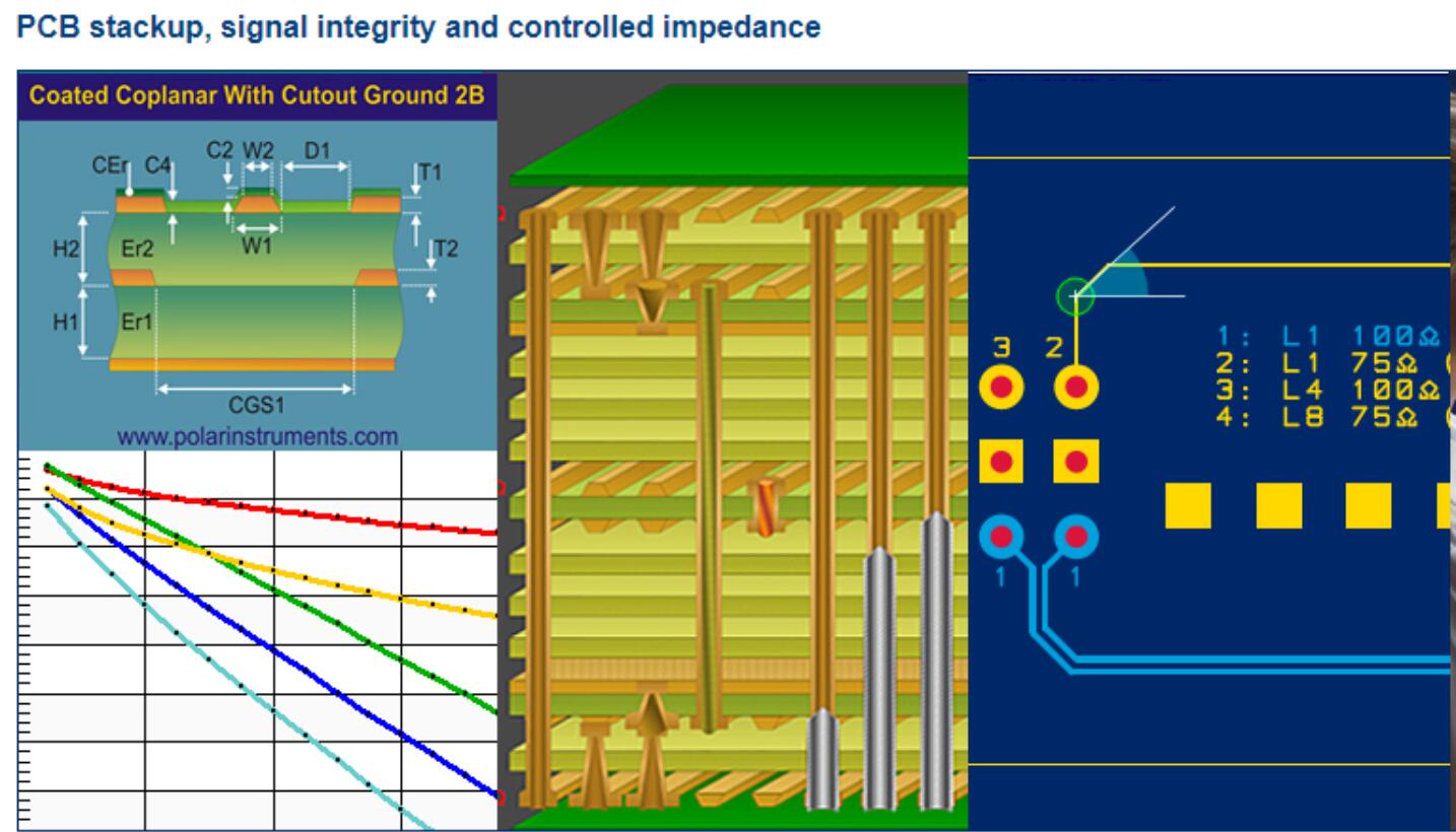
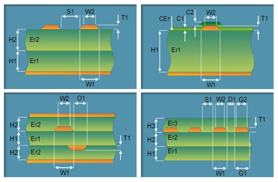
The characteristic impedance of a PCB trace is typically determined by its inductive and capacitive reactance, resistance, and conductance. These factors are a function of the physical dimensions of the trace, the dielectric constant of the PCB substrate material, and dielectric thickness. Typically PCB trace impedance can range from 25 to 125 ohms. The impedance value generated from the PCB structure will be determined by the following factors:
– Width and thickness of the copper signal trace (top and bottom)
– Thickness of the core or prepreg material on either side of the copper trace
– Dielectric constant of the core and prepreg material
– Distance from other copper features
How to Calculate Impedance Control?
Determining impedances on a PCB is important and requires some particular measurement methods. Let’s take a look at some impedance control measures that are credible, accurate, and reliable.
Smith Chart
The Smith chart was around before computers or PCB designing software was prevalent. The chart is used to describe the relationship between source and load impedance with the help of graphics. It also relies on an array of mathematical calculations to give an impedance value for a particular trace.
Computer Simulation
The software of today uses complex technology to determine control impedance numbers. The benefit of these programs is that they can merge your design considerations into a simulation to see a virtually finished product. However, this software is typically expensive to buy and use for modeling a finished PCB design.
Online Impedance Calculator
Online calculators are much more efficient and widespread than design software with PCB impedance control features. You can find out the controlled impedance for a trace through these calculators. These calculators are not as precise as the simulators, but you always get a ballpark figure to get the process rolling. Minor tweaking afterward can keep you safe because most of these calculators use standard numbers from the design guides for high-speed impedance boards.
All three methods listed above provide a good starting place for your calculations. No matter which method you adopt, you start with a safe set of rules compared to no impedance calculation.

Applications of controlled impedance
Controlled Impedance should be considered for PCBs used in fast digital applications such as:
– Telecommunications
– Computing 100MHz and above
– High Quality Analog Video
– Signal Processing
– RF Communication
An Introduction to the Design and Manufacture of Impedance Controlled PCBs. When board traces carry signals containing high frequencies, care must be taken to design traces that match the impedance of the driver and receiver devices.
The longer the trace, or the greater the frequencies involved, then the greater the need to control the trace impedance. The PCB manufacturer controls the impedance by varying the dimensions and spacing of the particular trace or laminate. For these reasons, a PCB designer will specify trace impedance and tolerance, and should work with the PCB manufacturer to ensure that the PCB meets the specifications for their Impedance Controlled PCB requirements.
Impedance is the sum of the resistance and reactance of an electrical circuit expressed in Ohms. The resistance being the opposition to current flow present in all materials. The reactance is the opposition to current flow resulting from the effect of the inherent capacitance and inductance of the conductor interacting with changes in voltage and current. In DC circuits there is no reactance and the resistance of copper conductors is typically insignificant. However, in high speed AC circuits (those with sharp changes in voltage and/or current) the reactance and thus the impedance can become very significant. This can become critical to a design’s functionality because of the effects that changes in the impedance along the signals path from transmitter to receiver will have on the efficiency of power transfer as well as signal integrity. While a circuit’s speed is often expressed as the frequency of the wave form: the critical concern is the speed at which the voltage and/or current is required to change.
Impedance Control PCB Manufacturing
To meet the growing demand for impedance control PCB, PCB manufacturers have invested a lot of money and workforce and material resources in production technology to meet the production requirements of customers.
Due to the difficulty of impedance control PCB production, PCB manufacturers generally require PCB designers or purchasers to provide more detailed information and requirements, such as the type of material needed, copper weight and thickness of the board, the number of layers, Gerber file, so that the manufacturer can prepare the bill of materials (BOM). Impedance information should be marked in the Gerber file. If the necessary information is lacking, even a little critical information will make it difficult or impossible for the manufacturer’s engineers to know exactly what the customer needs.
Impedance-controlled PCBs are also divided into three different situations:
No Impedance Control:
This is a situation where you do not need any extra design elements to ensure correct impedance because you have very loose impedance tolerance. Naturally, this will result in a faster-completed, less expensive board because the manufacturer does not have to include any special measures.
Impedance Watching:
What is impedance watching? This is a situation where the designer will outline the impedance control trace, and the PCB provider adjusts the trace width and dielectric height accordingly. Once the manufacturer approves these specifications, they can begin to manufacture the board. You can request a Time Domain Reflectometry (TDR) test to confirm the impedance for a fee.
Impedance Control:
Actual impedance control is something you will typically only request when your design has tight impedance tolerances that could be tough to hit the first time around. When the capability limits of the manufacturer get close to the dimension requirements, it can be tough to ensure target impedance on the initial attempt.
In the case of impedance control, the manufacturer makes the circuit board achieve the target impedance as far as possible. Then they tested TDR to see if they succeeded. If not, they adjust accordingly and try again until they reach the required impedance.

 Chinese
 English
 Russian
 Spanish
 Portuguese


