PCB Stencil
What is PCB stencil?
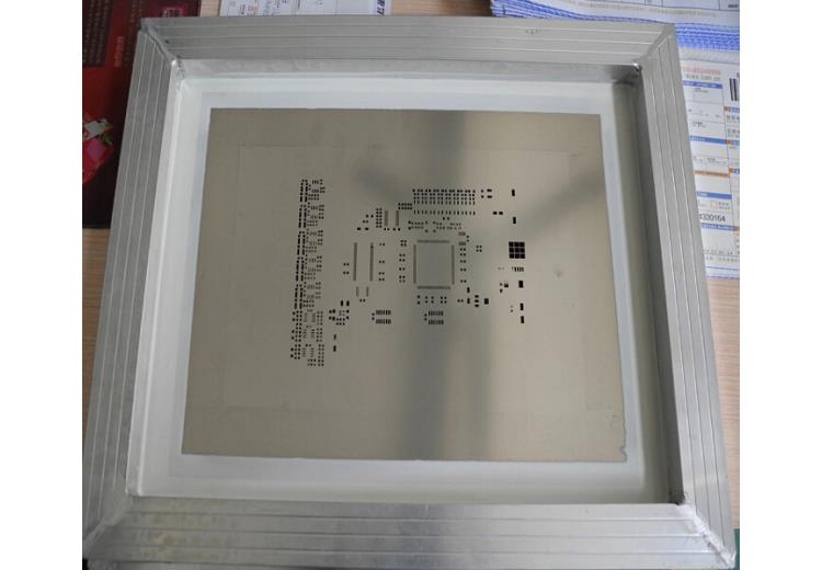
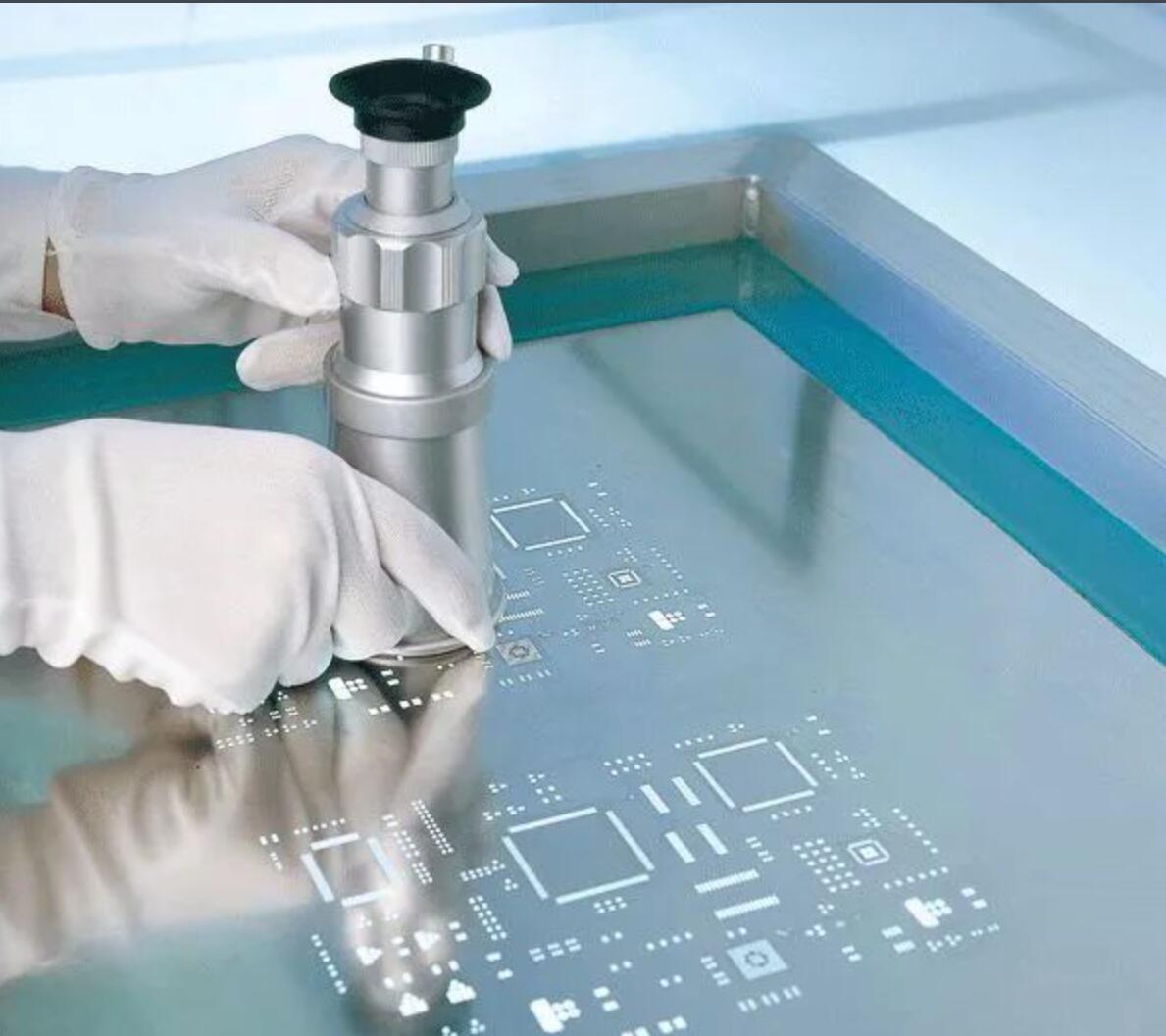
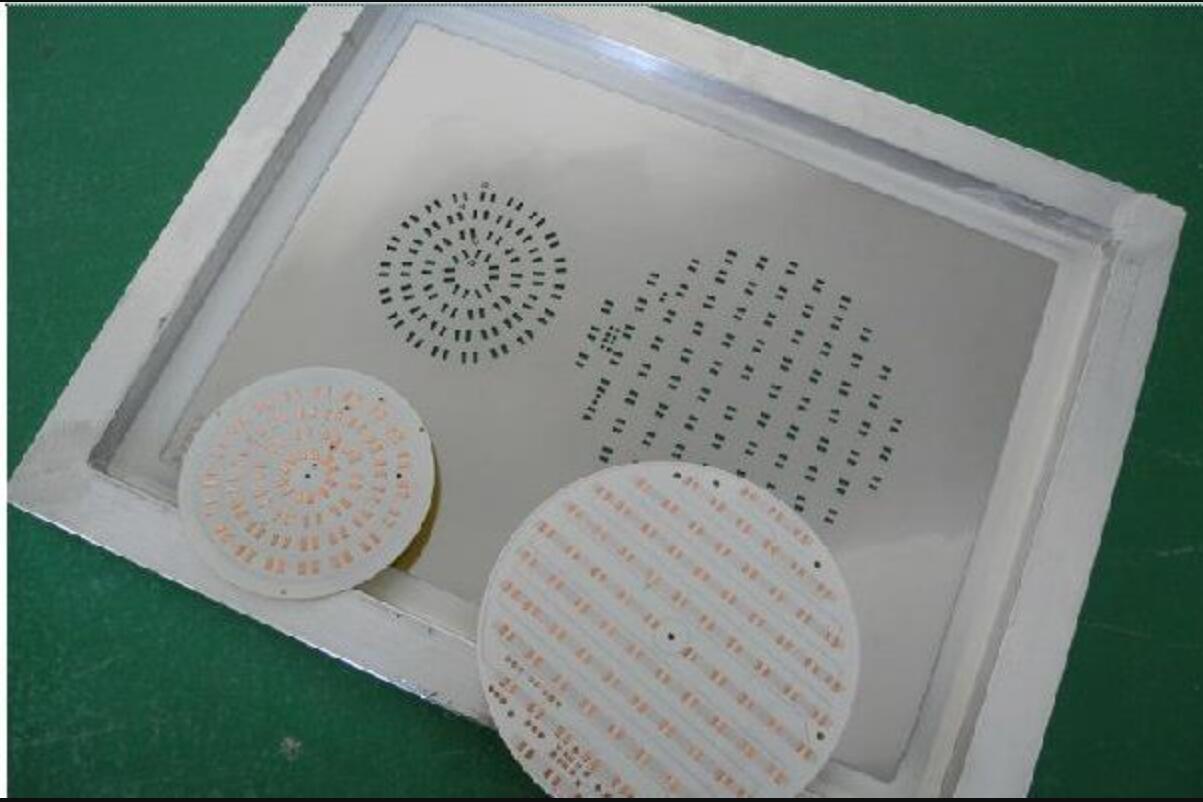
By definition, it infers to the stainless steel sheet comprising of laser-cut openings deployed in placing solder paste on printed circuit boards. It is instrumental for SMT or surface-mount technology, especially on component placement. The stencil’s primary use entails the deposition of solder paste to designated spots on a bare circuit board. Solder paste deposits then allow components to get placed and aligned on the printed circuit board.
Printed circuit boards are vital elements of electronics. But to have them, an intricate production process must happen first. A vital element of the design, fabrication and assembly process of electronic circuit boards entails the development of a PCB stencil. It is instrumental in determining where the solder paste gets located on bare PCB boards before component mounting. However, most PCB enthusiasts pay little to no attention to PCB stencils. So what does it imply, what is its importance to the PCB production process?
A PCB stencil needs to deposit the exact amount of solder paste precisely on the designated spot. It is vital as it ensures the pad-to-component solder joint provides the required mechanical strength and electrical connection. The use of a relevant PCB stencil in applying solder paste ensures a faster PCB assembly process. It also makes it simpler and precise.

Printed circuit board stencils get classified according to the mounting style and aperture type. As a result, the diverse PCB stencils include the following. Laser-cut stencils framed printed circuit board stencils, hybrid PCB stencils, and chemical-etch stencils. Other stencil types encompass frameless PCB stencils, etc. Such PCB stencils get offered by most PCB houses, including Hitechpcb PCB and Assembly. You can also get customized stencils based on your PCB design needs.
SMT Stencil or Surface Mount Technology Stencil is a fine laser-cut stainless-steel sheet, ideal for using in PCB assembly. The PCB stencil helps in transferring the solder paste with precision and accuracy.
Therefore, the SMT stencil technology is important for applying solder paste. As you know, applying the solder paste is a time taking task that requires delicacy and attention to detail. Choose Hitech Circuits’ SMT Stencil service, we have our own SMT stencil equipment with professional capabilities.
PCB stencil is very important. In the process of PCB Assembly, the printing quality of PCB solder paste stencil will directly affect the processing quality of SMT, and the quality of solder paste printing is directly related to the quality of PCB stencil, so the correct design SMT stencil, the selection of the appropriate PCB stencil thickness and the design opening size of the PCB stencil, will be the key to ensuring the printing quality of the solder paste.
The key factors that affect the quality of PCB stencil are PCB stencil material and PCB stencil thickness, PCB stencil opening type, PCB stencil size, PCB stencil wall flatness. Therefore, in the PCB stencil design, Processing, inspection, and production process must pay special attention to PCB stencil.
Types of the PCB Stencil
The Framed PCB/SMT Stencil
It comes as a solder paste stencil that is laser-cut and gets permanently mounted on the stencil frame. Mounting the solder paste stencil deploys the mesh border, which tightly stretches your stencil foil within a frame. Your framed stencils by design apply to high volume PCB screen printing. The stencil also has a smooth aperture, which can get applied for 16-Mil pitches or below.
Features of Framed SMT Stencil
1. It has a distinct process for the smooth aperture walls
2. An incredible print performance
3. Clean laser-cut openings or apertures
4. It is perfect for stencil printing targeting high-volume on PCBs
5. The unique process develops permanent (non-fading and non-removal) fiducial marks
6. All the framed surface-mount technology stencils get double bonded with intention to withstand extreme wear
8. It has a standard twenty-four hour turnaround period

How to select SMT Stencil?
1. Required minimum spacing and hole size.
2. The release paste performance of the template.
3. Reduce and prevent bridging, short circuits, or tin shortages of solder paste.
4. Cost, yield, and the cycle of processing materials.
5. The lifetime and durability of the template material.
6. Required solder paste thickness.
The stencil was originally made of wire mesh, so it was called a mask. It started with nylon polyester mesh, and later, due to its durability, it switched to wire mesh and copper wire mesh. Now it is stainless steel wire mesh. But no matter what material the wire mesh is made of, it has the disadvantage of bad shape and low precision. With the development of SMT technology, the requirement for SMT Stencil is higher and higher. SMT Stencil is coming into being. Stainless steel Stencil replaces them, which is now SMT Stencil.
The main function of PCB Stencil is to assist in the deposition of solder paste and to transfer the exact amount of solder paste to the exact location on the bare PCB. PCB Stencil consists of a mesh frame, wire mesh, and steel sheet. There are many holes in the steel sheet, which correspond to the location on the PCB where printing is required. During use, place the PCB under the PCB Stencil and leak the paste onto the PCB through the holes in the fixed position on the PCB Stencil.
How to use PCB stencil?
1. PCB samples or PCB batches will become bare PCB boards. Next, we need to welding circuit board.
2. Cover the PCB steel mesh onto the PCB.
3. Print the solder paste on the surface of the PCB optical disc by SMT laser stencil.
4. Print the solder paste and mount the SMT device.
5. The pasted PCB is soldered by reflux soldering-overheating oven-semi-solid solder paste.
6. Bare PCB boards are now semi-finished PCBA products.
SMT Stencil is a "delicate" precision mold, so be careful when using it:
1. Handle lightly;
2. Wash (wipe) Stencil before use to remove dirt carried during transportation;
3. Stir the paste or red glue evenly to avoid blocking the openings;
4. Optimal printing pressure: best pressure when the scraper just scrapes out the paste (red gel) on the Stencil;
5. It is best to use sticker printing when printing.
6. When the scraper has finished its journey, it is best to stop for 2-3 seconds before demolding, if possible, and the molding speed should not be too fast.
7. Do not hit PCB Stencil with hard objects or sharp knives;
8. Clean PCB Stencil after use and return to the box and place it on a special storage rack.
Laser Cutting
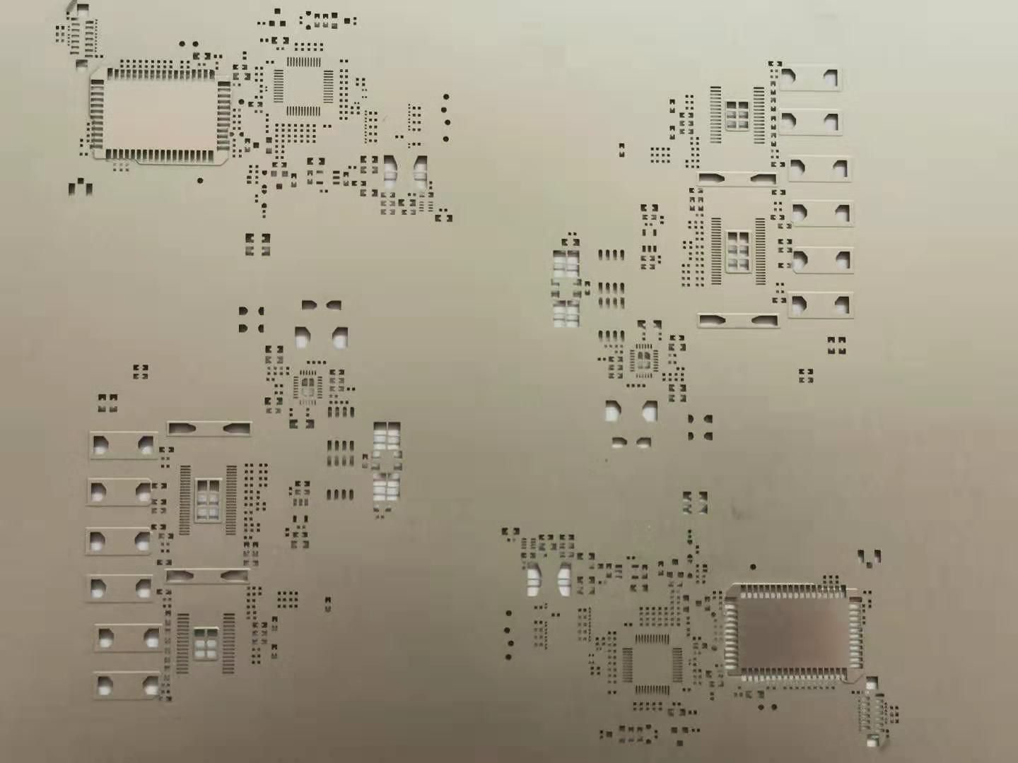
It also comes as a subtractive procedure where the stencil foil material gets removed through laser cutting. Laser cutting by default often leads to a finer output and assists in realizing greater accuracy. It also leads to a more consistent output or results compared to the process of chemical etching. However, it is prudent to note that the process is independent of the chemical environment and thus does not need moisture protection.
Benefits of a Laser Cut Stencil
Tapered slots
It is quicker compared to other stencil-making processes like chemical etching.
Absence of film tooling
Drawbacks of the Laser-Cut Stencil
The aperture’s sidewalls come rough
It requires an extra deburring process

SMT stencil prices are calculated mainly by the following requirements:
1. Opening process, including etching, laser, ionic cascade, depends on the accuracy of the stencil opening and the product's process requirements. The cheapest and least accurate etching is also the lowest. Laser cutting of stencil is generally required for spacing less than 0.35mm.
2. Stencil thickness, different stencil thickness price is also different, in addition to the thickness process with special requirements, such as chemical staircase stencil price is higher.
3. Size, of course, the larger the size, the more expensive it is.
4. Material, Stencil border thickness dimensions, protective coating, etc.
5. Other requirements, such as single-sided network, double-sided network, and so on, vary in price.
Guidelines of Designing a PCB Stencil
If you want to realize reliable and sturdy solder joints in your printed circuit board, it becomes necessary to print a stencil design. The aperture or opening size when it comes to the adjacent pad stencil has a direct correlation to the stencil’s thickness. But it is possible to design thicker stencils with a smaller opening to that of the pad size. On the other hand, thinner stencils can also get designed with aperture size to a stencil thickness ratio of 1:1. The recommendation, however, entails deploying a laser to ensure the steel mesh possessing apertures and electro-polishing.
Some of the design guidelines to consider, however, include the following.
The Adjacent Pad’s Stencil Design
The stencil’s thickness determines the quantity of solder paste that gets printed onto the printed circuit board. Plenty of solder paste results in bridging during the process of reflow soldering, and this often proves undesirable. Because of this, industry recommendations entail the QFN package of 0.5mm pitch to deploy a 0.12mm steel mesh thickness. On the other hand, the QFN package with the 0.65mm pitch needs to deploy a 0.15mm steel mesh thickness. However, it is possible to design the stencil’s aperture relatively smaller than the pad size. It reduces incidences of solder bridging.
Heat Dissipation Pad Design of the PCB Stencil
The exposed pads’ soldering at the chip’s bottom to the PCB’s thermal pads can lead to air holes. It results as the gas located inside the large-size pads and thermal vias overflow outwards during the soldering process. It means, therefore, that whenever the solder paste spot or area proves too enormous, incidences of defects like solder balls and sputtering occur. But it is impossible to get rid of the pores means refocusing and limiting the pore size. It would help if you also took the necessary precaution by considering the aspects needed when designing the thermal pad of the stencil.
Always develop numerous small apertures in the thermal pad area instead of a single large aperture or opening. A common value bandied around includes 50% to around 80% of solder paste treatment or coverage. Additionally, the thickness of the solder joint needs to fall at 50μm, going by the industry practice and outcomes. It helps enhance the board-level reliability. An incredible way of realizing this thickness entails ensuring at least 50% solder thickness at the under-fill thermal vias. However, for the through-hole, the rate of coverage needs to range above 75%.
Importance of a PCB Stencil in the Assembly Process of Printed Circuit Boards
The conventional form of the assembly process of printed circuit boards entailed manual placing of electronic components before soldering. But the ever-increasing complexity of electronic circuit boards, besides the need for miniaturization, has necessitated a machine-operated component placing and solder paste application aided by SMT stencils. It is no longer viable to place and solder numerous small components on smaller circuit boards.
In the assembly process of printed circuit boards, solder paste has to go in the designated spots. Such spots denote the areas electronic components have to get soldered within the conductive path of the board. While manual soldering would otherwise make sense for simple circuit designs involving a few components, complex ones need a more elaborate approach. It is necessary to ensure fewer inconsistencies from human mistakes besides proper alignment and functionality of the PCB.
PCB stencils make repetitive solder impressions and act as templates to guide the solder paste application on the PCB. It gets placed and aligned correctly on the PCB. A runner then moves across the PCB stencil screen while squeezing the correct proportions of the solder paste through the circuit board holes.

Benefits
Solder paste stencils make it possible to work faster, more accurately, besides making the work more straightforward.
PCB stencils also reduce the amount of labor and time in assembling printed circuit boards which translates to a faster time-to-market scenario of products.
It also guarantees a tremendously fine pitch precision when it comes to printing.
Printed circuit board stencils also assist in the reduction of errors and defects when printing, including ultra-fine pitch board patterns.
Stencils are instrumental in the uniform application of solder across all the surface-mount device pads.
It also ensures high pad positional precision.
The Step-Down and Step-Up Stencil Aspect
SMT production demands sophisticated approaches, especially in complex and challenging circuits with components like ceramic BGAs, small components, or RF shields. Other mass-produced techs like the Internet of Things (IoT) require such advanced levels of complexity. However, it also has the overriding importance of cutting down on cost and saving time. Components that need different solder paste volumes get placed closer to avert instances of voltage surges or ESD.
It is a type of assembly that needs a different set of approaches beyond the aperture dimensional adjustment. The need to connect various sized components and cleaner while ensuring optimal transfer efficiency implies deploying stencils possessing varied foil thicknesses. The approach gets referred to as a step-down and step-up stencil. It allows for the adjustment of different quantities of the solder paste on the same circuit board. It also includes the clean application of solder paste around elevated spots or areas.
The Step-down and step-up stencil approach only has a ten-year history since its inception. However, the technology has become an effective method of integrating different or mixed parts/components requiring varying paste requirements. Step stencils prove valuable in streamlining the assembly time besides lowering the assembly costs. It arises because step areas or spots can get replaced, which allows for reusing of the stencils.
Application of Step-Down and Step-Up Stencil
Step-up areas apply in instances where a large volume besides the height of the solder deposit proves necessary. On the other hand, step-down areas limit the height and volume of the solder. Step-less areas or steps utilize ramped areas to accommodate big or large components, especially those needing more paste deposits. Step-relief cavities cater to board irregularities like bar codes or raised areas. Angled steps, however, reduce the damage that arises from the squeegee.
Components with small footprints like 0201 have to vary their solder paste volumes to avert incidences of short-circuiting. It may not become possible to vary the width and length of the tiny fixed area, though varying the height can prove the ideal solution.
Besides accommodating a mix of components with low and high paste requirements, it has other application areas. It includes realizing co-planarity when it comes to components with different heights. It also encompasses the printing of PCBs with separate surface elevations or stickers. Step-down and step-up stencils should have a standard 0.5mm minimum distance between the component pad and the step’s edge.
The crucial factors influencing the step stencil’s efficiency include the squeegee angle, speed, pressure, direction, and material. Additionally, the distance between the step’s edge to the nearest opening or aperture also influences the efficiency of the step stencils. However, it is prudent to ensure the stencil design optimizes the solder deposits for every electronic component. Too much or too little solder paste has adverse effects on the functionality of the stencil and ultimate impact on the printed circuit board assembly.
The manufacturing process of PCB stencil has a great influence on the printing quality of the solder paste. Which PCB stencil to use depends on the product characteristics, size of welded terminals, component type, and component distribution of components on the PCB board.
Final Thoughts
A PCB stencil is instrumental in the fabrication and assembly process of printed circuit boards. Every PCB design engineer or enthusiast needs to understand the different types, their corresponding importance, and their application in their PCB development process. Additionally, finding the right partner for your PCB assembly needs helps get a suitable PCB solder paste stencil for your circuit board assembly essentials.

0086-755-29970700
sales@hitechpcb.com; sales@hitechcircuits.com
2F, Building C, Suojia Technology Park, Hangcheng, Bao’an, Shenzhen, Guangdong, China 518126
 Chinese
 English
 Russian
 Spanish
 Portuguese


