RF PCB & Microwave PCB
What is RF PCB & Microwave PCB?
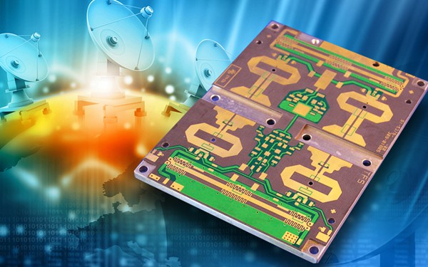
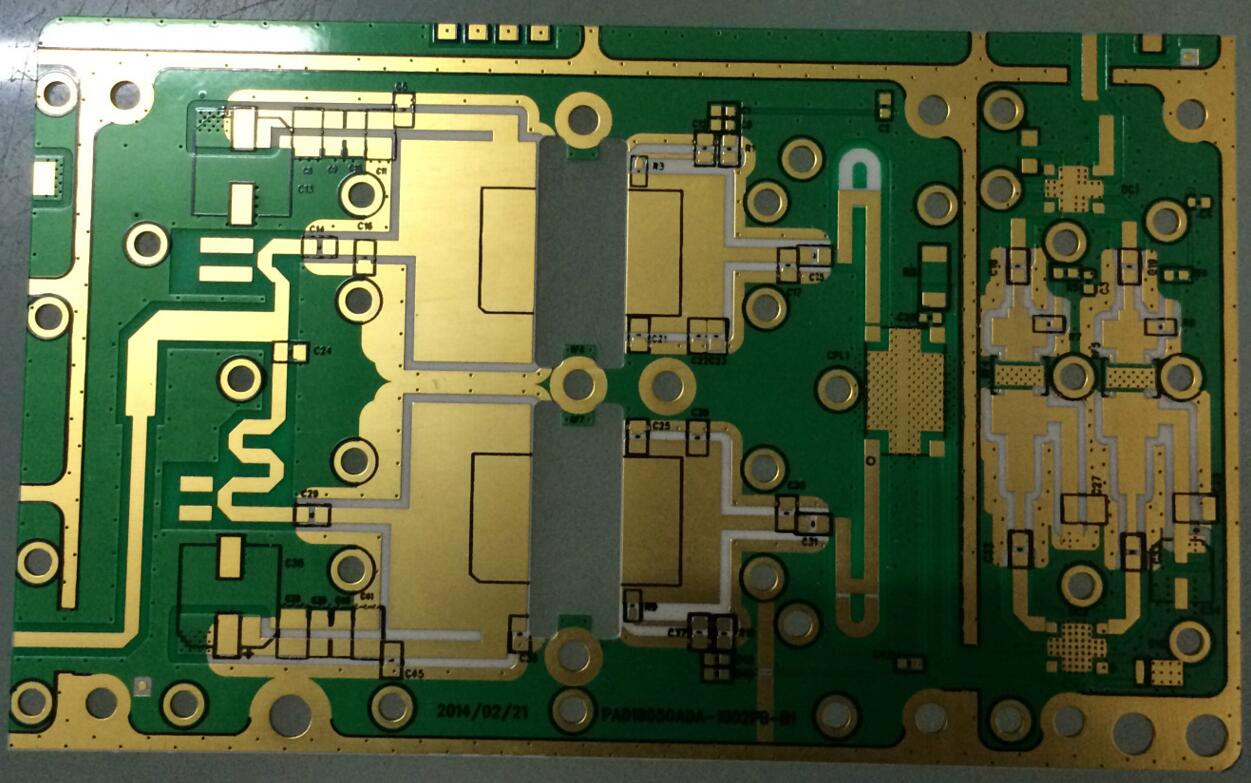
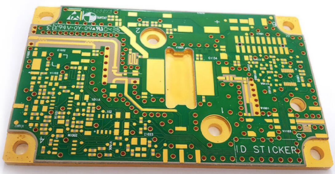
RF PCB and microwave PCB are a type of printed circuit boards which carry the RF or microwave signal. So, these types of PCBs usually work on megahertz to gigahertz frequency ranges. Hence, we use these frequency ranges in communication technologies from mobile phones to radars.
The materials used are advanced composites with very specific characteristics for dielectric constant (Er), loss tangent, and CTE (co-efficient of thermal expansion). These materials can be mixed in the same Stack-Up for optimal performance and economics.
The advantages of using materials with a low X, Y and Z CTE is a resulting PCB structure that will remain extremely stable in high temperature environments while operating at up to 40 GHz in analog applications, allowing for the effective placement of very fine pitch components including, in some cases, bare die-attach.
RF is Radio Frequency, a signal with a very high frequency. The choice of circuit board substrate depends on the requirements for the performance indicators of the circuit board. It can be ordinary FR4 epoxy glass fiber or a special microwave substrate such as Teflon, Arlon, Rogers materials.
As complexity of electronic components increases, the one thing that becomes imperative is signal rates and high frequency of transmission. Little surprise then that the demand for high frequency PCBs is on the rise. They find use in a variety of high-speed design applications that require a frequency range of 500MHz to 2GHz.

FR-4, based on epoxy resin and glass reinforcement, is the most popular laminate material for printed circuit board industry for a long time. The FR4 dielectric constant ranges from 3.8 to 4.8, depending on the glass weave style, thickness, resin content, and copper foil roughness. However, PCB industry also use other material for different application. In RF/microwave products, low loss and special controlled dielectric constant material like PTFE (Teflon) was widely used. These material was developed long time ago. Partly because of low volume in production, it is quite expensive in the past. When wireless became popular in consumer products years ago, the demand for low loss material was went high. But the material cost is still high. Even some new developed material were trying to get involved, it seems none of them can reduce the material cost dramatically. How to reduce the RF PCB cost became an essential problem for the designer. One of the solution is the mixed dielectric design.
Because the low loss material is not needed for all wireless system, it mostly designed-in, from my understanding, for the circuits from antenna to power amplifier. To reduce the PCB cost, designer used multiple PCB and only the front end of the receiver subsystem need high cost low loss material. However, the cost is still high because of multiple PCB’s and the connector between them. Beside, the Teflon PCB is soft and is comparably difficult in assembly due to warpage.

RF PCB standard:
1. Low power RF PCB mainly uses standard FR4 material (good insulation properties, uniform material, dielectric constant ε=4, 10%).
2. In the RF PCB design, each component should be closely arranged to ensure the shortest connection.
3. For a mixed-signal PCB, the RF and analog parts should be far away from the digital part (the distance is usually more than 2cm, at least 1cm), and the ground of the digital part should be separated from the RF part.
4. When selecting components to work in a high-frequency environment, use SMD(Surface Mounted Devices) as much as possible. SMD are small in size, and the component pins are generally very short.
This article provides guidelines and suggestions for radio frequency (RF) printed circuit board (PCB) design and layout, including some discussion of mixed-signal applications, such as digital, analog, and RF components on the same PCB. The content is organized by topic areas and provides “best practice” guidelines, which should be applied in conjunction with all other design and manufacturing guidelines. These guidelines may also apply to specific components, PCB manufacturers, and materials.
High Frequency PCB Features
1. The impedance control requirements are more stringent, the relative line width control is very strict, the general tolerance is about 2%.
2. Due to the special plate, the adhesion of PTH to copper is not high. It is usually necessary to roughen the via and surface by means of plasma processing equipment to increase the adhesion of PTH hole copper and solder resist ink.
3. Can not be used before the resistance welding, otherwise the adhesion will be very poor, can only be roughened with micro-etching water.
4. Most of the plates are made of PTFE. There are many burrs formed by ordinary milling cutters, and special milling cutters are required.
5. The high-frequency PCB is a special circuit board with a high electromagnetic frequency. Generally, the high frequency can be defined as a frequency above 1 GHz.
6. Its physical properties, precision, and technical parameters are very high, and it is often used in automotive anti-collision systems, satellite systems, radio systems and other fields.
7. In general terms, the PCB industry considers an RF circuit board to be any high frequency PCB that operates above 100MHz. Within the radio frequency class, anything above 2GHz is a Microwave PCB.
Benefits of RF PCB & Microwave PCB
1. RF circuit board and microwave PCB board can work on high Frequencies.
2. They have a stable structure. Hence, it allows them to work at high temperatures.
3. These have a stable dielectric constant and a low loss tangent. So, the signal travels through them with minimum impedance.
4. It is possible to form a multilayer board stack up. Hence, we can make smaller boards. Therefore, they give optimal performance and are cost-effective.
5. They allow for fabricating complex layouts. So, it is easier to assemble fine pitch components onto the board.
Microwave PCB and High Frequency PCB–Common Problems and Solutions
RF circuit boards, and Microwave PCBs, are especially difficult to design compared to traditional PCB layouts. This is due to the problems that could arise in receiving or transmitting the radio signals. Some of the main problems are noise sensitivity, and tighter impedance tolerances
Compared to traditional circuit boards, radio and microwave signals are very sensitive to noise and also require much tighter impedance tolerances. The best solution for these problems is to utilize ground plans and use a generous bend radius on impedance controlled traces. These solutions will ultimately allow the RF/Microwave PCB to achieve the best performance.
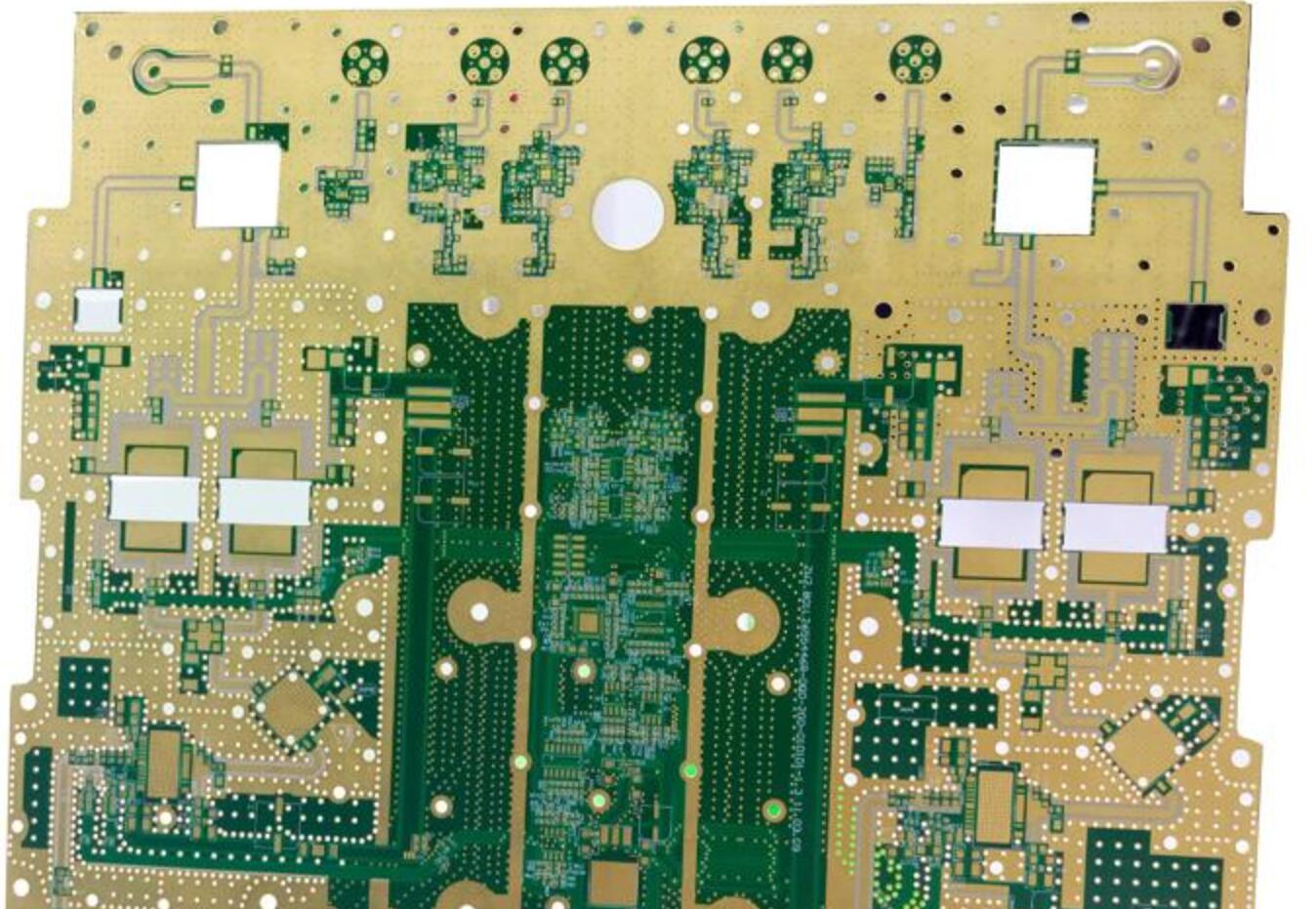
The manufacture of mixed dielectric Hitech Circuits has been quite standard for many PCB fabricators. The difficulty in manufacturing is to get an optimum production parameter for two or more different materials. Since most of the design is not balanced in construction, the warpage problem need to be carefully managed. It relates to material choice and design as well as the lamination process. Sometimes, use the exotic material on the bottom layer to balance the design can be a solution. But usually it’s not necessary and only bring a lot of cost.
To meet electrical performance, the mixed dielectric multilayer is designed with blind/buried via quite frequently. In some case, it can bond with metal and used in the power amplifier application.
The application for the mixed dielectric Hitech Circuits is not only for high frequency products. For high speed digital design, it may also help. For example, if there are some critical transmission lines need to pass long distance in PCB and the Df (dissipation factor) of FR-4 material is too high and cause signal integration problem, use some low loss material in part of the inner layer may have great help. It can save some cost instead of using low loss PCB material in all layers.

Application of RF PCB & Microwave PCB
RF PCB & Microwave PCB & High Frequency PCB uses materials of excellent dielectric property for its main body with other dielectric materials and metal substrates matched to complete corresponding multi-layer processing or thick-film processing and manufacture and to achieve the transmission functions of excellent high thermal conductivity, low dielectric constant, high frequency and high speed.
RF PCB are widely used in microwave transmission, Automobile telephone, radar antenna, wireless networks, Automotive Radar, wireless communications and satellite microwave communications, in particular the popularity of 5G networks exacerbate the market demand for the product on the RF PCB.
In order to meet increasing demands of Microwave PCB & RF PCB for our customers all around the world, we have increased investment and intensity of research & development on Microwave high frequency PCB over the last few years. We're now experienced in professional production of various high-frequency circuit boards from quick turn prototypes to production run. For most of RF PCB materials, such as: Ceramic PCB, Teflon PCB, Rogers PCB, Taconic PCB, Arlon PCB, we have sufficient inventory to ensure fast delivery.
Finding perfect RF Microwave PCB for your project can be stressful especially when it comes to choosing suitable PCB material. For a project developer, it is of great interest that his PCB may be of high-grade material with proper functioning and it should be delivered in time.
The parameters such as RF Microwave energy levels, Operating frequency, operating temperature range, Current and Voltage requirements are of great importance when choosing perfect material for PCB material.
When getting started with your PCB manufacturing, make sure you have chosen the right specifications for your PCB. Classical High-frequency RF Microwave frequencies were single layer PCB constructed on the dielectric. However, with the evolution in RF Microwave PCB designs, many technologies have emerged during the past few decades.
Why do you need to focus on choosing the right manufacturer?
Ordering PCB manufacturing from a high tech equipped facility can be more beneficial than getting it manufactured in a low-cost manufacturing facility with low-grade material used.
RF PCBs are highly sensitive towards factors such as noise, impedance, electromagnetism, and ESds. High-quality PCB manufacturers focus on eliminating any affecting factors during manufacturing. A poor quality RF Microwave PCB is not expected to sustain for long, and that’s why choosing a perfect RF PCB manufacturer can alter your product experience.
Today, most of the modern RF PCB manufacturing facilities use Computer Aided Engineering software simulation programs for PCB manufacturing. The best advantage of CAD-based RF Microwave PCB manufacturing is that it has simulation models of various brands and PCB models with proper product specifications.
These parameters are essential in the production of a standardized RF Microwave PCB and ensure reliability. Furthermore, the machines also support manual functioning, allowing the operator to perform manual operations.
So, it is evident that RF Microwave PCB manufacturing is not as simple as it seems.

Why choose Hitechpcb for your RF Microwave PCB manufacturing?
HITECH CIRCUITS has been providing RF PCB manufacturing facilities for years. The qualified professionals at HITECH CIRCUITS have expertise in Rogers PCB materials based PCB manufacturing. Fortunately, HITECH CIRCUITS has experienced RF Microwave PCB manufacturing for communication equipment.
HITECH CIRCUITS has specialized in Rogers PCB materials and prefers it for RF Microwave PCB manufacturing. The diverse range of Rogers PCB materials allows us to choose the most suitable material according to requirements.
HITECH CIRCUITS has been dealing in RF PCB manufacturing facilities for diverse products all over the globe. The qualified professionals at HITECH CIRCUITS have expertise in Rogers PCB manufacturing. Fortunately, HITECH CIRCUITS has experienced RF Microwave PCB manufacturing for communication equipment.
The material used in m equipment for PCB assembly was Rogers 4003c, Rogers 4350 and RT5880. This SMT based dual layer assembly incorporated 350 deployments. The final product was tested at an automated x-ray and optical equipment. The quality assurance department thoroughly examined each product. The products were delivered after complete satisfaction of multiple departments.
Since HITECH CIRCUITS has been into PCB product development and with a diverse experience of assisting project developers from various fields, Hitechpcba has developed a long-lasting relationship with its satisfied clients.
One of the primary reasons why you should consider HITECH CIRCUITS is its technical support always available just a few clicks away. Hitechpcb technical team is always available for technical support. If you are looking for a manufacturing company that will help you through out your RF PCB manufacturing process and will share ideas and strategies for your product development, you should consider Hitechpcb.

0086-755-29970700
sales@hitechpcb.com; sales@hitechcircuits.com
3F, B5 Dong, Zhimeihuizhi, FuYong, Bao’an Dist. Shenzhen, GuangDong, China 518103
 Chinese
 English
 Russian
 Spanish
 Portuguese


