PCBA Testing
What is PCBA Testing?
PCBA testing refers to the test of electrical conductivity and input-output value based on PCBA board with electronic components.
PCBA SMT processing is very complicated and includes multiple important processes, such as PCB board manufacturing process, component procurement and inspection, SMT assembly, DIP, and PCBA testing. Among them, PCBA testing is the most critical quality control step in the entire PCBA processing process. The testing determines the final performance of the product.
In the design of PCB, there is a numerical relationship between different test points, such as voltage and current. However, the process flow of PCBA production and processing is very complex, including many important processes such as the PCB manufacturing process, component procurement, and inspection, SMT patch assembly, dip plug-in PCBA test. In the process of production and processing, various problems may occur due to improper equipment or operation. Therefore, it is necessary to use professional test equipment or a manual multimeter to test the test points, To verify whether the actual PCBA Board meets the design requirements and ensure that each product will not have quality problems.
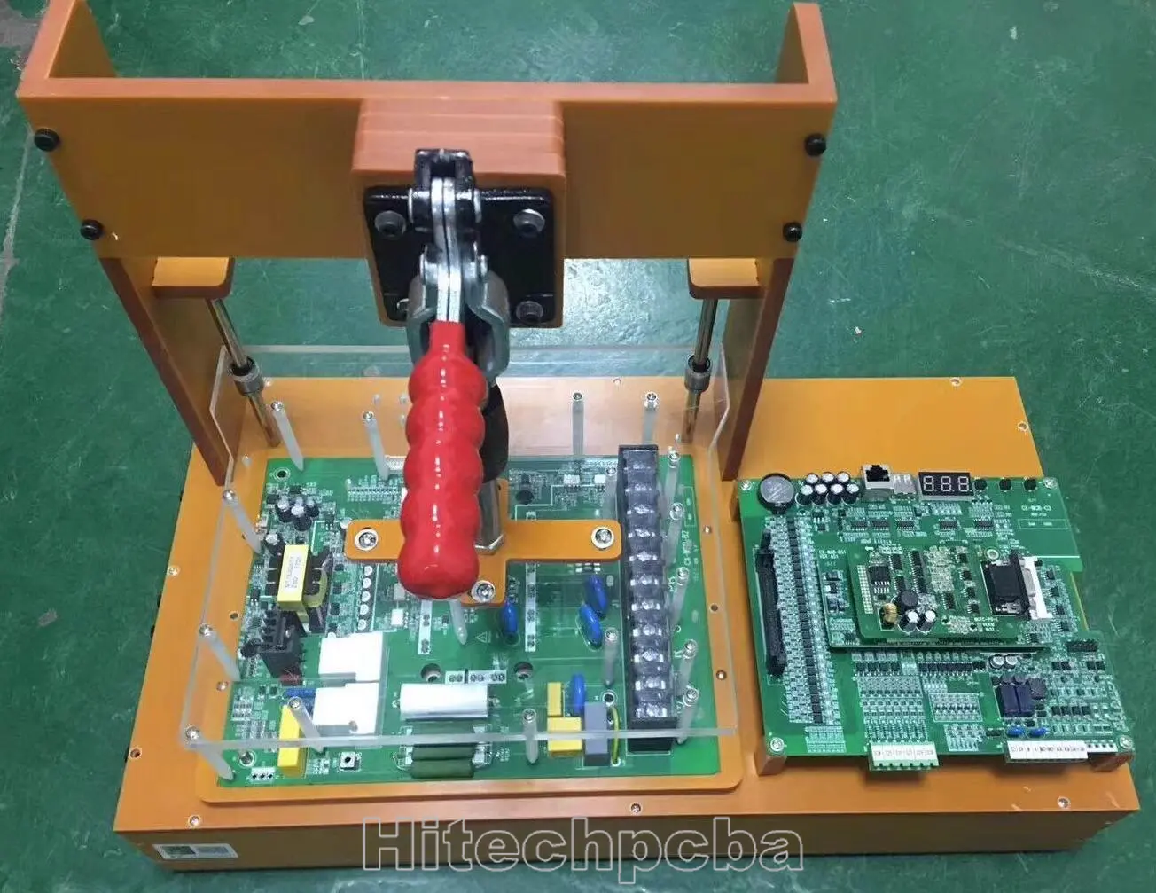
PCBA testing is a key step to ensure the quality of production and delivery. FCT test fixture is made according to the test point program and test steps designed by customers, and then the PCBA board is placed on the FCT test rack to complete the test.
Testing is crucial to ensure high quality products are delivered to customers. Thankfully board assemblers offer multiple layers of testing and inspection to ensure high-quality, assembled Circuit boards are produced and delivered to customers. Despite all efforts to prevent errors, printed circuit board assembly is a complex process and defects sometimes occur relating to a variety of issues from incorrect component loading to failures in SMT equipment. Thorough testing and inspection occurs throughout the production process to ensure problems are captured early on, ensuring high quality and yield.

Visual Inspection of Solder Paste
Visual inspection is a vital element in ensuring problems are captured and corrected as early in the process as possible, reducing the time and cost associated with rework and wastage. Visual inspection begins with the solder application. Inspection at this stage checks for correct deposition of solder paste on pads to ensure components reflow properly. Here testing helps prevent solder bridges, open circuits or fragile joints prone to failure.
Pre and Post Reflow Inspection
Pre and post reflow inspection are important elements in quality control. Pre-reflow inspection catches placement errors at a point where they are easy to repair, avoiding repetitive mistakes early in the process. This is important with products like automotive boards where regulatory compliance require that boards cannot be reworked. Components and boards are heat sensitive and detection of errors at this stage can avoid their damage or destruction. Post-reflow inspection can be manual or with AOI.
A ‘first article’ inspection is performed on a run to ensure all SMT feeders are set up correctly and that there are no issues like worn vacuum nozzles or alignment of the vision system. Board assemblers can offer a special ‘First Article Service’ that enables a rapid and cost effective pre-production process by expediting a production of a few boards to designers for testing prior to a full run.
Post reflow BGA inspection and testing, along with other leadless parts require special considerations as the component package shadows solder joints making inspection impractical without special equipment. Inspection can be conducted by a range of devices including: computed-tomography (CT) scanning, specially angled optics microscopes, endoscopes and X-ray machines.
Flying Probe Testing
Flying probe testing is good for where a PCB testing is prohibitively expensive. Flying probe has relatively low setup cost and a test procedure can be designed and implemented in a single day. Assembled PCBs with all components placed are compared electrically against the measurements from a golden board for verification. It can conduct open, short, orientation and component value circuit checks. This can help verify correct component placement and alignment.
For PCB assembly, in order to ensure high quality, we do and provide related testing and inspection, include:
1.Manual Test
Manual testing is to directly rely on visual inspection to confirm the placement of components on the PCB assembly. This method is widely used. However, there are many components in the PCBA, and most of them are very small, which makes this method less applicable. Some functional flaws are not easy to detect, and data cannot be easily collected. Due to this, more professional testing methods are needed.
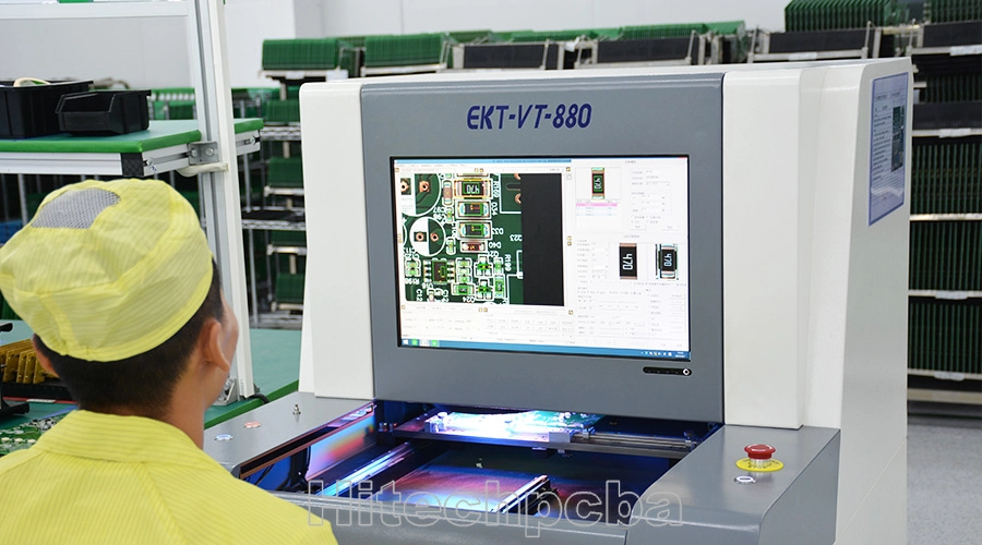
2.Automatic Optical Inspection (AOI)
Automatic optical inspection, also known as automatic visual inspection, is carried out by a special inspection instrument and is used before and after reflow. It has a relatively good effect on the polarity inspection of components and is a common method. But this method is more difficult in identifying a short-circuited PCBA.
3.Flying Probe Test
The flying probe testing has been generally welcomed in the past few years due to advancements in mechanical accuracy, speed, and reliability. The test system’s current requirements include fast conversion, low-volume manufacturing, and no fixture capabilities required for prototype manufacturing, making the flying probe testing the best choice.
4.Function Test
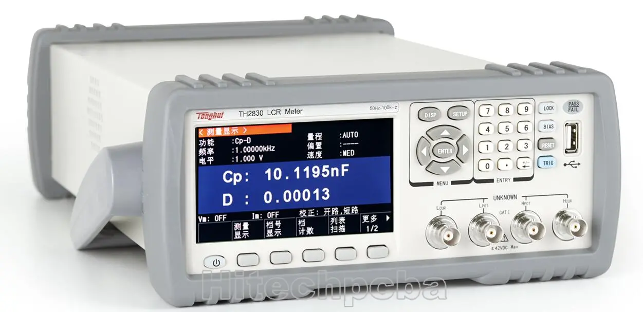
This is a test method for a specific PCB or unit, which is done by special equipment. Functional testing mainly includes the final product test and the latest entity model (Hot Mock-up).
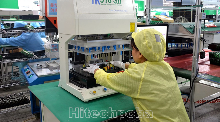
5.Manufacturing Defect Analyzer (MDA)
This test method’s main advantages are low initial cost, high output, easy follow-up diagnosis, and fast and complete short circuit and open circuit tests. The disadvantage is that the test cannot detect functional problems. There is usually no test coverage indication, fixtures must be used, and the test cost is high.

How to test the PCBA board?
1. PCBA board manual test
Manual testing is to test directly by the vision and confirm the component mounting on PCB through vision and comparison. This technology is widely used. However, the large number and small components make this method more and more unsuitable. Moreover, some functional defects are not easy to be found, and the data is not easy to collect. In this way, more professional testing methods are needed.
2. PCBA board automatic optical inspection (AOI)
Automatic optical testing, also known as automatic visual testing, is carried out by a special tester. It is used before and after reflow and has a good effect on the polarity inspection of components. Easy-to-follow diagnosis is a common method, but this method is poor in short circuit identification.
3. PCBA board flying needle tester
Needle testing has been widely welcomed in the past few years due to advances in mechanical accuracy, speed, and reliability. In addition, the requirements for the test system with fast conversion and fixture-free capability required for prototype manufacturing and low-yield manufacturing make the flying needle test the best choice.
4. PCB Assembly board function test
This is the test method of a specific PCB or a specific unit, which is completed by special equipment. Functional tests mainly include final product tests and hot mock-up.
5. PCB Assembly manufacturing defect analyzer (MDA)
The main advantages of this test method are low initial cost, high output, easy-to-follow diagnosis, fast and complete short circuit, and open-circuit test. The disadvantage is that the function test cannot be carried out, there is usually no test coverage indication, the fixture must be used, and the test cost is high.
What is the testing principle of PCB Assembly by fixture?
PCB Assembly testing is a key step to ensure the quality of production and delivery. It refers to making FCT test fixtures according to the test points, procedures and test steps designed by customers, and then placing the PCBA board on the FCT test fixture to complete the test process. The test principle of PCBA is that: connect the test points on the PCBA board through the FCT test fixture(frame) to form a complete path, then connect the computer and the program tool (programmer), and upload the MCU program. The MCU program will capture the user’s input action (such as long pressing the switch for 3 seconds), and control the on-off of the adjacent circuit (such as LED flashing) or drive the motor to rotate through calculation. By observing the voltage and current values between the test points on the FCT test fixture, and verifying whether these input and output actions are consistent with the design, and so, the test of the entire PCBA board would called completed.
Want to know more? Contact me at sales@hitechpcb.com

How about bare PCB testing? Please refer to it as below.
When you order printed circuit boards (PCB), you know the pricey consequence of failure. The last thing you need financially is for your PCBs to suddenly drop dead -- or to have a shortened life span because of a design or QA issue.
PCB assembly testing methods are an integral part of the manufacturing process. Reputable electronics contract manufacturers (ECMs) offer a variety of PCB testing methods, but the seven main types include:
In-circuit testing
Flying probe testing
Automated optical inspection (AOI)
Burn-in testing
X-Ray inspection
Functional testing
Other functional testing (solderability, contamination, and more)
Here’s a primer on the most important types of PCB testing. This should prepare you better for discussions with your ECM:
7 TYPES OF PCB TESTING METHODS
1. IN-CIRCUIT TESTING
In-circuit testing (ICT) is the most robust type of PCB testing in existence. The high price reflects that -- tens of thousands of dollars, though the cost will depend on board and fixture size, among other factors.
An ICT, also known as a bed-of-nails test, powers up and actuates the individual circuitry on the board. In most cases, the test is designed for 100% coverage, but you’ll get closer to 85-90% coverage. The nice thing about ICT is that the 85-90% you get is totally free of human error.
This test involves using fixed probes laid out in a way that matches the design of the PCB. The probes checks the integrity of the solder connection. The bed of nails tester simply pushes the board down on the bed of probes to start the test. There are access points predesigned in the board that allows the ICT testing probes to make connections with the circuit. They put a certain amount of pressure on the connection to make sure it stays intact.
ICT is often performed on bigger connections and ball grid arrays (BGAs).
This test is for a “mature” product with very few revisions expected. If you don’t have design-for-manufacturing as part of your goal, with the proper pads on the board, you may not be able to use an in-circuit test. Unfortunately, you can’t change your mind and move to an ICT strategy halfway through production.
2. FLYING PROBE TESTING
Flying probe testing is a tried-and-true option that’s less expensive than in-circuit testing. It’s a nonpowered type of test that checks for:
Opens
Shorts
Resistance
Capacitance
Inductance
Diode issues
The test works through the use of needles attached to a probe on an x-y grid obtained from basic CAD. Your ECM programs coordinates to match the circuit board and then runs the program.
We touched on flying probe vs. ICT being a common comparison. Each has advantages and disadvantages.
In some cases, ICT makes it unnecessary to use flying probe testing, but the PCB has to be designed to fit with the test fixture -- which means a higher initial cost. ICT can be faster and less error-prone than flying probe testing, so you might find the extra cost is worth it. While flying probe testing can be cheaper initially, it may actually be less cost-effective for large orders.
One final word of caution: A PCB flying probe test does not power up the board.
3. AUTOMATED OPTICAL INSPECTION (AOI)
AOI uses either a single 2D camera or two 3D cameras to take photos of the PCB. The program then compares the photos of your board to a detailed schematic. If there is a board that does not match the schematic to a certain degree, the board is flagged for inspection by a technician.
AOI can be useful for detecting issues early to ensure production is shut down ASAP. However, it does not power up the board and may not have 100% coverage for all part types.
Never rely solely on an automated optical inspection. AOI should be used in conjunction with another test. Some of our favorite combos are:
AOI and flying probe
AOI and in-circuit test (ICT)
AOI and functional testing
4. BURN-IN TESTING
As the name suggests, burn-in testing is a more intense type of testing for PCBs. It’s designed to detect early failures and establish load capacity. Because of its intensity, burn-in testing can be destructive to the parts being tested.
Burn-in testing pushes power through your electronics, usually at its maximum-specified capacity. The power is run through the board continuously for 48 to 168 hours. If a board fails, it is known as an infant mortality. For medical applications, boards with high infant mortality are clearly not ideal.
Burn-in testing isn’t for every project, but there are some cases where it makes a lot of sense. It can prevent embarrassing or dangerous product launches before they reach customers.
Just remember that burn-in testing can shorten the product’s lifespan, especially if the test puts your board under more stress than it’s rated for. If few or no defects are found, it's possible to reduce the testing limit after a shorter period to avoid over-stressing your PCBs.
5. X-RAY INSPECTION
Also referred to as AXI, this type of “testing” is really more of an inspection tool, at least for most ECMs.
During this test, an X-ray technician is able to locate defects early during the manufacturing process by viewing:
Solder connections
Internal traces
Barrels
There are 2D and 3D AXI tests, with 3D offering a faster testing period.
X-ray testing can check elements that are usually hidden from view, such as connections and ball grid array packages with solder joints underneath the chip package. While this check can be very useful, it does require trained, experienced operators.
Also, note that your ECM can’t necessarily inspect every layer of a board using an X-ray machine. It’s true we can see through the board to detect internal defects, but it’s a very time-consuming and expensive process (for both ECM and customers).
6. FUNCTIONAL TESTING
There are customers who do like a good, old-fashioned functional test. Your ECM uses this to verify that the product will power up.
This test does require a few things:
External pieces of equipment
Fixtures
Requirements for UL, MSHA, and other standards
This functional test and its parameters are usually provided by the customer. Some ECMs can help develop and design such a test.
It does take time. If you want to get your product out the door quickly, this may not be your best choice. But from a quality and longevity standpoint, functional testing can save face and save money.
7. OTHER FUNCTIONAL TESTS
There are other types of functional tests that can be used to check your PCB, depending on the circumstances.
A PCB functional test verifies a PCB’s behavior in the product’s end-use environment. The requirements of a functional test, its development, and procedures can vary greatly by PCB and end product.

Other PCB assembly testing types include:
Solderability test: Ensures surface sturdiness and increases chances of forming a reliable solder joint
PCB contamination testing: Detects bulk ionics that can contaminate your board, causing corrosion and other issues
Micro-sectioning analysis: Investigates defects, opens, shorts, and other failures
Time-domain reflectometer (TDR): Finds failures in high-frequency boards,
Peel test: Finds the measure of strength required to peel the laminate from the board
Solder float test: Determines the level of thermal stress a PCB's holes can resist
Advantages of functional PCB testing include:
Simulates the operating environment, minimizing customer cost
May eliminate the need for expensive system tests
Can check product functionality -- anywhere from 50% to 100% of the product being shipped, your need to check and debug it
Pairs well with other tests, such as ICT and flying probe
Great for detecting incorrect component values, functional failures, and parametric failures
CONSIDER YOUR CIRCUMSTANCES
Figuring out what PCB testing is right for you can be a challenge; there are certainly a lot of methods! Your ECM will know which tests are right for your specific needs, so consult with them often.

0086-755-29970700
sales@hitechpcb.com; sales@hitechcircuits.com
2F, Building C, Suojia Technology Park, Hangcheng, Bao’an, Shenzhen, Guangdong, China 518126
 Chinese
 English
 Russian
 Spanish
 Portuguese


