What is Multilayer Printed Circuit Board?
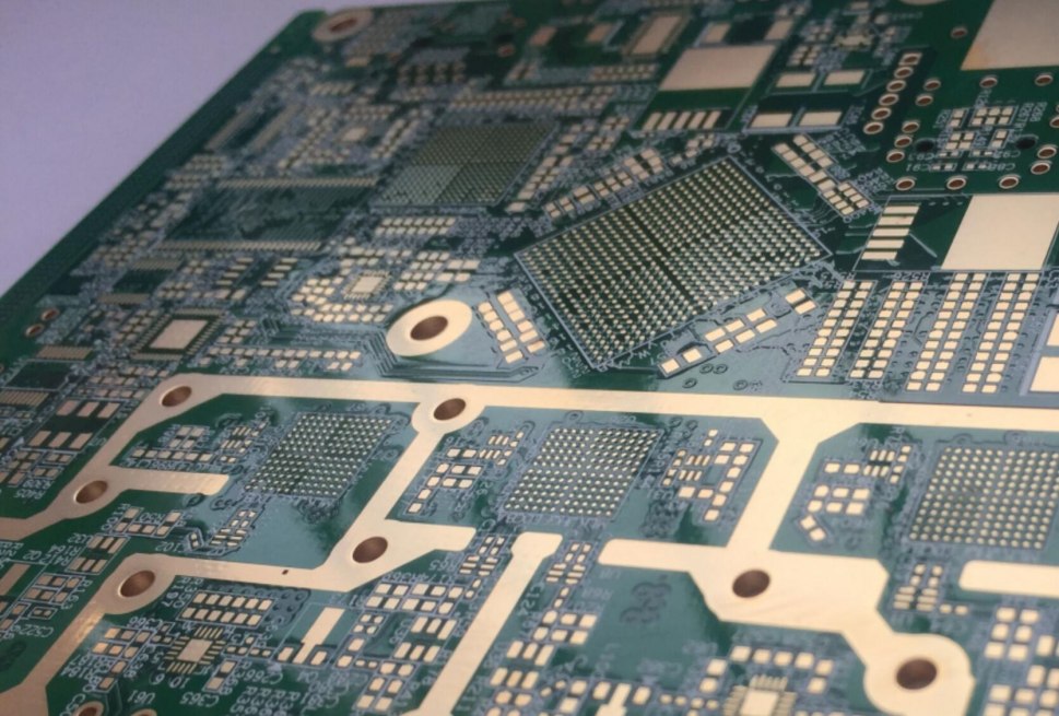
-The printed circuit board determines the difficulty and processing price of the process according to the amount of the copper layers. The normal PCB is single -sided and double -sided, but high-end electronic products, due to product space design factors restrictions, in addition to dividends outside the surface wiring, multi-layer lines can be superimposed inside. During the production process, after making each layer of lines, then the optical equipment positioning and pressing together, so that the multi -layer lines are superimposed in a printed circuits board. Commonly known as Multilayer printed circuit board. All PCB greater than or equal to 2 layers can be called a multi-layer PCB. Multi-layer circuit boards can be divided into, multi-layer rigid PCB, multi-layer flex PCB, multi-layer rigid-flex PCB.
-What is Multilayer Printed Circuit Board?
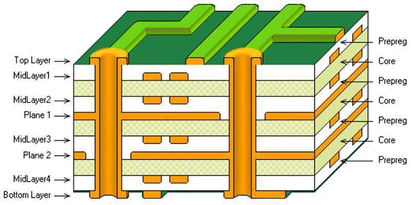
The definition of multilayer PCB is a PCB made of three or more conductive copper foil layers. They are displayed as several double -sided circuit boards and stick to the thermal insulation layer with them. The entire structure is arranged so that the two layers can be placed on the surface of the PCB to connect to the environment. All electrical connections between layers are implemented through Vias, such as vias shops that are blind and buried through holes. The application of this method then generates a highly complex PCB.
Multilayer PCB is attributed to changes in the continuous development of the electronics industry. Over time, the function of electronic devices has gradually become more complicated and requires more complicated PCB. Unfortunately, PCB is restricted by problems such as noise, strange capacitors, and skewers, so it is necessary to follow some design constraints. These design precautions make it difficult to obtain satisfactory performance level from a single or even double-sided PCB . Therefore, multilayer PCB is born.

Multilayer PCB packages the power of doubled-layer PCB into a small part of the size, which is becoming more and more popular in electronic products. They have various sizes and thickness to meet the needs of its continuous expansion applications. The variant range ranges from four to twelve layers. The most commonly of the layer has an even number, because the odd number layers may cause problems such as distortion in the circuit, and no longer have cost-effective production. Most applications require four to eight layers. Although applications such as mobile devices and smartphones tend to use about twelve layers, and some professional PCB manufacturers have the ability to produce nearly 100 layers of PCB. However, multilayer PCB is rare because they cost higher.
Although they do tend to produce more expensive and dense labor, multilayer PCB is becoming an important part of modern technology. This is mainly due to the many benefits they provide, especially compared with single-layer and double-layer varieties.
-Multilayer PCB Benefits
The assembly density is high, the volume is small, and the quality is light. Due to the high assembly density, the connection between each component (including components) is reduced, so it improves reliability; it can increase the number of wiring layers and increase the flexibility of design; A certain impedance circuit; the high-speed transmission circuit can be formed; the circuit and magnetic circuit shielding layer can be set, and the metal core heat dissipation layer can be set to meet the needs of special functions such as shielding and heat dissipation; it is simple and highly installed and high.
• Small size: One of the most prominent and praise of the multilayer PCB is its size. Due to its layered design, multilayer PCB is essentially smaller than other PCB with similar functions. This brings great benefits to modern electronic products, because the current trend is working hard to achieve smaller, more compact, and more powerful small tools, such as smartphones, laptops, tablets, and wearable devices.
• Light Construction: The weight of smaller PCB is lighter, especially because the multiple connectors required by a single single chain and double -layered PCB are eliminated, which is conducive to multilayer design. Third, this is good for modern electronics, which is more suitable for mobility.
• High quality: Since the work and planning of multilayer PCB must be participated in, these types of PCB quality is often better than single-layered and double-layered PCB. Therefore, they also tend to be more reliable.
• Expensation of durability: Multilayer PCB is often durable. These multilayer PCB must not only bear their weight, but also be able to deal with the calories and pressure that bind them together. In addition to these factors, the multilayer PCB uses the multilayer insulating layer between the circuit layer to combine it with the pretreatment adhesive and the protection material.
• Enhanced flexibility: Although this is not suitable for all multilayer PCB components, some do use flexible construction technology, which leads to flexible multilayer PCB. This may be a very desirable feature for applications that may occur with mild curvature and bending semi -periodic. Similarly, this is not suitable for all multilayer PCB, and the more layers in the flexible PCB are mixed with layers, the smaller the flexibility of the PCB.
• More powerful: Multilayer PCB is a very high density component that incorporates multiple layers into a single PCB. These close -range wooden boards can be more connected, and their congenital electrical properties make them smaller, but their capacity and speed are higher.
• Single connection point: Multilayer PCB is designed as a single unit, not connected to other PCB components. As a result, they have a single connection point instead of using multiple connection points required to use multiple single-layered PCB. It turns out that this is also the benefit of the design of electronic products, because they only need to include a connection point in the final product. This is particularly beneficial for small electronic products and small tools that aim to minimize size and weight.
-Multilayer PCB Disadvantages
High cost; Long Lead time; High reliability detection methods. Multilayer Pinting Crcuit Borads is a product developed to the development of high-speed, multifunctional, large -capacity, and small volume direction. With the continuous development of electronic technology, especially the widespread and in -depth application of large -scale and large -scale integrated circuits, multilayer printing circuits are rapidly developing in high density, high precision, and high-level digital directions. Technologies such as blind holes and other technologies to meet the needs of the market.
• higher cost: At each stage of the manufacturing process, multilayer PCB is much more expensive than single-layered and double-layered PCB. They are difficult to design and spend a lot of time to solve any potential problems. They also need a highly complex manufacturing process to produce, which requires a lot of time and labor. In addition, due to the nature of these PCBs, any errors in the process of manufacturing or assembly are difficult to rework, resulting in additional labor costs or waste costs. The most important thing is that the equipment for multilayer PCB is very expensive because it is still a relatively new technology. Because of all these reasons, unless the size is absolutely necessary for applications, cheaper alternatives may generally be a better choice.
• Complex production: Multilayer PCB is more difficult to produce than other PCB types, and requires more design time and careful manufacturing technology. This is because even small defects in PCB design or manufacturing may make it useless.
• Limited availability: One of the biggest problems of multi -layer PCB is to produce the mechanical costs they need. Not all PCB manufacturers have the funds or necessity of this mechanical, so not all PCB manufacturers carry it. This limits the number of PCB manufacturers that can produce multilayer PCB for customers. Therefore, it is best to ask the PCB manufacturer's ability carefully to determine it as a contract manufacturer.
• Need to be proficient designer: As mentioned earlier, multilayer PCB needs to be extensive in advance. Without previous experience, this may be a problem. Multilayer boards require interconnection between layers, but they must reduce the problems of string and impedance at the same time. A problem in the design may lead to non-function boards.
• Production time / Leadtime: As the complexity increases, manufacturing requirements are more. This is the key issue of the turnover rate of every multilayer PCBs of directors requires a lot of time to produce, resulting in more labor costs. In addition, it may lead to a longer period of time between orders and when the product receives, which may be a problem in some cases.
-Advantages of Multilayer PCBs over Single Layer Alternatives
The multilayer PCB is a printed circuit board made of alternate conductive graphics layer and insulating material layer. The number of layers of conductive graphics is more than three layers, and inter-layer electrical connection is achieved through metallic holes. If one double-sided panel is used as the inner layer, two single-panels as the outer layer or two double panels as the inner layer and two single-piece panels as the outer layer, the positioning system and insulating bonding material are overlapped together, and the conductive graphics are pressed and pressed by the conductive graphic. The design requirements for interconnection have become four-layered and six-layered printed circuit boards, also known as multilayer Printed Circuit Boards.

Compared with the production process of general multilayer boards and double panels, the main difference is that the multilayer board adds several unique process steps: inner imaging and blackening, layer pressure, concave erosion, and drilling. In most of the same process, some process parameters, equipment accuracy and complexity are also different. For example, the inner metallic connection of multilayer plates is a decisive factor for the reliability of multilayer boards. The quality requirements for the wall of the hole are stricter than the double -layer board, so the requirements for drilling are higher. In addition, the number of stacked boards of each drill each time and the speed and feed of the drill bit during drilling are different from the double panel. The inspection of multilayer and semi-finished products is also rigorous and complicated than double panels. Due to the complex structure, the multilayer board should use uniformly temperature glycerin hot-melt process without using infrared hot-melt process that may cause excessive local temperature to rise.
-PCB Manufacturing Services
As a PCB manufacturer in China, HITECH CIRCUITS provides PCB manufacturing services, and supplies consistent quality and affordable price of printed circuit boards globally. No matter it is PCB prototyping or PCB production project, we can meet your PCB fabrication needs in a variety of PCB materials and technologies.
HITECH CIRCUITS focuses on multilayer boards, impedance-controlled PCBs and HDI boards in varying complexities. We conduct 100% DRC checks for your designs when receipt of your Gerber files and PCB fabrication drawings to ensure the best quality possible circuit boards will be delivered on time.

0086-755-29970700
sales@hitechpcb.com; sales@hitechcircuits.com
2F, Building C, Suojia Technology Park, Hangcheng, Bao’an, Shenzhen, Guangdong, China 518126
 Chinese
 English
 Russian
 Spanish
 Portuguese


