What is Heavy Copper PCB?
What is the Heavy Copper PCB?
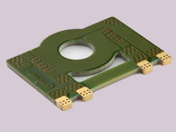
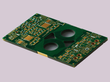
Heavy Copper PCB belongs to a special process, with a certain technical threshold and operating difficulty, the cost is relatively expensive, in FR-4 layer bonding a layer of copper foil, when the completion of copper thickness ≥2oz, defined as Heavy Copper PCB board. Heavy Copper PCB has very good extension performance, is not limited by the processing temperature, high melting point can be used oxygen blowing, low temperature is not brittle and other hot melt welding, and also fireproof, belongs to non-combustible materials, Heavy Copper PCB thickness is different, the specific application occasions are also very different.
Heavy Copper PCB high temperature resistance, corrosion resistance, mainly used in the products with power savings, especially need to run high voltage and current electronic products is the need for Heavy Copper PCB. Heavy Copper PCB needs multi-layer screen printing and multi-layer welding and multi-layer copper plating, Heavy Copper PCB because of the use of PCB and signal of the current size and thickness of the different, complete copper thickness ≥2oz plate called Heavy Copper PCB, 2oz finished copper thick, manual printing a screen printing is not enough to fill the gap between the lines, must be printed two welding resistance. When PCB production meets 2oz and thicker, it will be noted in the resistance: Heavy Copper PCB, need two screen printing, in order to achieve no redness of the line, the line surface negative welding thickness is greater than 10um. Copper plating generally includes primary copper, secondary copper, and primary copper. The main purpose of primary copper plating is to provide sufficient copper thickness for secondary copper etching, so as to ensure that the copper thickness after secondary copper etching can meet the customer's standard requirements.
Hitech Circuits currently offers 1-32 layers of PCB fabrication with samples up to 28oz copper thickness, batch sizes up to 10oz, minimum laser borehole 0.1mm and minimum mechanical borehole 0.15mm.

2. Performance and advantages of Heavy Copper PCB
Heavy Copper PCB has the characteristics of carrying high current, reducing thermal strain, and good heat dissipation. Not limited by the processing temperature, high melting point can be used oxygen blowing, low temperature is not brittle and other hot melt welding, and fire prevention, belongs to non-combustible materials. Even in extremely corrosive atmospheres, copper sheet forms a strong, non-toxic passivation protective layer.
The advantage of Heavy Copper PCB
Heavy Copper PCB is widely used in various home appliances, high-tech products, medical and other electronic equipment. The application of Heavy Copper PCB makes the circuit board, the core component of electronic equipment products, have a longer service life, and also helps to simplify the volume of electronic equipment. The application field and demand of Heavy Copper PCB have been rapidly expanded in recent years, and it has become a kind of "hot" PCB variety with good market development prospects.
The vast majority of Heavy Copper PCB are plates with high current (current x voltage = power). The main application fields of Heavy Copper PCB are two main fields: power module (power module) and automotive electronic parts. Its main terminal electronic product areas, some of the same as the conventional PCB(such as portable electronic products, network products, base station equipment, etc.), and some of the conventional PCB areas, such as automotive, industrial control, power module, etc.
The high current substrate differs from conventional PCB in efficacy. The main function of conventional PCBs is to form the wires that carry information. And the large current substrate is a large current through the substrate, bearing power devices, the main effect is to protect the carrying capacity of the current and make the power supply stable. The development trend of this kind of high-current substrate is to carry more current. The heat emitted by larger devices needs to be dissipated, so the large current passing through is larger and larger, and the thickness of all copper foil on the substrate is thicker and thicker. Now manufacturing high current substrate 6 Oz Heavy Copper has become routine.
3. Heavy Copper PCB silkscreen printing process
The anti-bright printing of Heavy Copper PCB is a necessary process for the production of Heavy Copper PCB, which can protect the outer circuit, so as to avoid the problems of oxidation of the outer circuit or welding short circuit. At present, screen printing is adopted in weld-proof printing, but there are certain difficulties in screen printing of Heavy Copper PCB. The production line generally adopts one printing, and the amount of oil is increased by adjusting the mesh mesh number and printing pressure. Due to the large thickness of the line copper, the traditional printing is difficult to ensure the quality, prone to line Angle ink thickness is insufficient or wrinkles between lines, bubble lines yellow and other problems. At the same time, there is also the production method of secondary printing, but many secondary printing needs to be baked twice, or it needs two silk screen printing machines for printing at the same time, and the cost is high. When the screen printing of Heavy Copper PCB, there will be uneven ink thickness, wrinkles, bubbles, yellow lines and other problems. So, what is the specific process of silk screen printing of Heavy Copper PCB? Heavy Copper PCB screen printing process includes the first printing, drying process and second printing in sequence.
The first printing: use a scraper to scrape the first oil, so that the first ink is transferred to the Heavy Copper PCB through the mesh provided with graphic part, forming the first layer of graphic. The first ink needs to add diluent, the quality of the diluent accounts for 1%-2% of the total quality of the ink.
Drying process: Place the Heavy Copper PCB printed with the first layer of text and text in a ventilated place for 15-30 minutes. This drying process requires the second printing at normal temperature: use a scraper to scrape the second ink, so that the second ink is transferred to the Heavy Copper PCB through the mesh with the text and text part, and form a second layer of text and text on the first layer of text and text. The second ink printing does not add diluent.
The silk screen printing method of Heavy Copper PCB also includes the post-baking process set after the exposure process. In order to make the ink solvent fully volatilized, the segment-type oven is used in the post-baking process to bake the Heavy Copper PCB step by step, so as to ensure the quality of Heavy Copper PCB. Heavy Copper PCB belongs to the special plate, Hitech Circuits is committed to providing customers with better PCB service, welcome to consult.
4. Heavy Copper PCB fine line etching
In the production process of PB Heavy Copper PCB, line punching is always a difficult point. In order to achieve his purpose, the production of general choice of multiple fast her moment or one-time slow moment. With the chip integration is getting higher and higher, PCB circuit board is also gradually developing in the direction of light, thin, short and small. The etching line width is getting smaller and smaller, and the current required to carry on the line is getting larger and larger. Therefore, the requirement of dry thickness is also increased from the original 10Z and 20Z to 30Z 40Z, which is more than 50Z and 6 Oz. During line etching, because of the complex copper, it is difficult for fresh etching liquid to enter, pool effect or the limitation of the capacity of its own equipment, Heavy Copper etching often becomes the difficulty of the process. Hitech Circuits is a professional manufacturer of Heavy Copper PCB circuit boards. We have summarized some suggestions on Heavy Copper PCB circuit board etching during the production process of Heavy Copper PCB circuit board etching.
a. When etching Heavy Copper PCB, more uniform etching line shape and etching factor can be obtained by repeated alternating etching without changing the production conditions.
b. Multiple etchings are equivalent to improved etching capability, that is, etching smaller spacing lines than one etching.
c. When etching Heavy Copper PCB, the direction of dense line length is taken as the etching direction, which can obtain better etching factor and line alignment.
d. Etching factor = etching line thickness /[(line width - line width)/2], which has reference value as an etching quality standard in Heavy Copper etching.
5. Heavy Copper PCB etching factor
Heavy Copper PCB wire is formed by chemical clock carving. Because the etching liquid is gradually etched from the surface of exposed copper to the interior, it is also etched horizontally to the side copper junction when it is etched vertically to the interior, forming the so-called etching side corrosion phenomenon. In order to quantitatively compare the etching quality of etched line, we define the etching factor, which is used as an index to quantitatively measure the etching quality and the etching ability of etched line. The actual calculation of etching factors has been a variety of understanding, Hitech Circuits to introduce the calculation method of Heavy Copper PCB etching factors?
There are two algorithms to calculate the engraving factor of PCB composite copper plate body. Method 1 is the result of some people's understanding of the clock engraving factor. The calculation method is based on the upper and lower width of the clock engraving line after the completion of the clock research process, and the specific calculation formula is etching factor = etching line thickness /[(lower width - upper width)/2. The test results of the calculation method show that the more over etching, the larger the etching factor. For normal etched 0.5 Oz thin copper plate, the calculated ton cutting factor is 2.5, while for excessive Heavy Copper PCB (1 Oz and 2 Oz), the cutting factor is as high as 5.6 and 6.0, which is a great difference. The formula of engraving factor calculation method 2 is etching factor = engraving thickness (anti-bell layer width - maximum line width) 2. The calculation of engraving factor in Method 2 covers three states of etching process: over-engraving, normal etching and under-engraving. The test results of using method 2 to calculate the etching factor show that the etching factor of normally etched thin copper plate is 2.7, while the etching factor of excessively etched Heavy Copper PCB is 2.3 and 2.0, respectively, with little difference. Therefore, it is suggested that the premise of calculating the etching factor should be in the normal etching state.

6. Application of Heavy Copper PCB
Heavy Copper PCBs have a number of benefits over standard PCBs. In addition, they offer excellent features that make them ideal for specific applications. For example, Heavy Copper PCBs are ideal medical devices, and many other fields. As a result, the demand for Heavy Copper PCB is increasing.
Here are some applications of Heavy Copper PCBs:
Solar energy converter
Track traction system
Nuclear power industry
Automobile industry
UPS system
Protective relay
Torque control
Safety and signal system
Welding equipment
Power line motor
7. What are the advantages of Heavy Copper PCB? Why do you choose Heavy Copper PCB?
Heavy Copper technology is one of the solutions to meet the needs of modern power electronics. Heavy Copper printed circuit boards are the latest trend in PCB industry. Heavy Copper PCBs are highly used in high power and current applications in power supplies, welding equipment, power distribution, power converters, solar panel equipment, medical, automotive, aviation and other fields because the Heavy Copper layer helps control heat dissipation and run high power and current. Our Heavy Copper PCB manufacturing services cover single - sided, double - sided and multilayer PCBs. In addition, Heavy Copper PCBs can be manufactured in FR4, polyimide, aluminum based, copper based, ceramic based and PTFE laminate materials.
Heavy Copper PCB, also known as Heavy Copper PCB, or high copper PCB. The thickness of copper on PCBs is usually discussed in terms of "thickness" in ounces. 5 ounces of copper means it's 175? M(7mils) thick. Measurements are made by spreading 1 ounce (28.35 g) of copper evenly over a 1 square foot (929cm2) PCB area. What is a Heavy Copper PCB? There is no standard definition. But when the thickness of the inner or outer copper layer is 2oz(ounces), 3 ounces per square foot or more, we consider it a Heavy Copper sheet.
What are the advantages of using Heavy Copper PCBs?
Electroplating and etching are combined to make the side walls straight and the bottom negligible.
Increase the copper thickness of PTH and sidewall.
Increase the conductivity range of the current.
Potentially smaller board sizes from layering.
Increase the strength of the connection.
Transfer heat to an external radiator.
Improve the mechanical strength of the joint and the PTH hole
Increase tolerance to thermal strain.
Add a high power density plane transformer onboard
8. What can Heavy Copper PCBs provide?
Heavy Copper PCBs have a lot to offer. It has some unique features that make it ideal for high-end applications. Let's discuss some of the benefits of this PCB;
• Great heat distribution: This PCB provides high thermal resistance due to its copper-plated through-hole. Heavy Copper PCBs are used in applications requiring high speed and high frequency. You can also use this PCB in harsh temperatures.
• Mechanical strength: Heavy Copper PCBs have very high mechanical strength. When used, this PCB makes the electrical system durable and rugged.
• Good conductor: Heavy Copper circuit boards are good conductors. Because of this property, they are used in the production of electronic products. They help hold the various plates together. These plates can transmit electricity.
• Onboard radiators: Heavy Copper PCB provide onboard radiators. Using these plates, you can achieve an effective radiator on a Mosaic surface.
• Large dissipation coefficient: Heavy Copper PCBs are ideal for large components with high power consumption. These PCBs prevent the electrical system from overheating. They dissipate heat effectively.

0086-755-29970700
sales@hitechpcb.com; sales@hitechcircuits.com
3F, B5 Dong, Zhimeihuizhi, FuYong, Bao’an Dist. Shenzhen, GuangDong, China 518103
 Chinese
 English
 Russian
 Spanish
 Portuguese


