PCB Assembly Cost
Cost of PCB Assembly
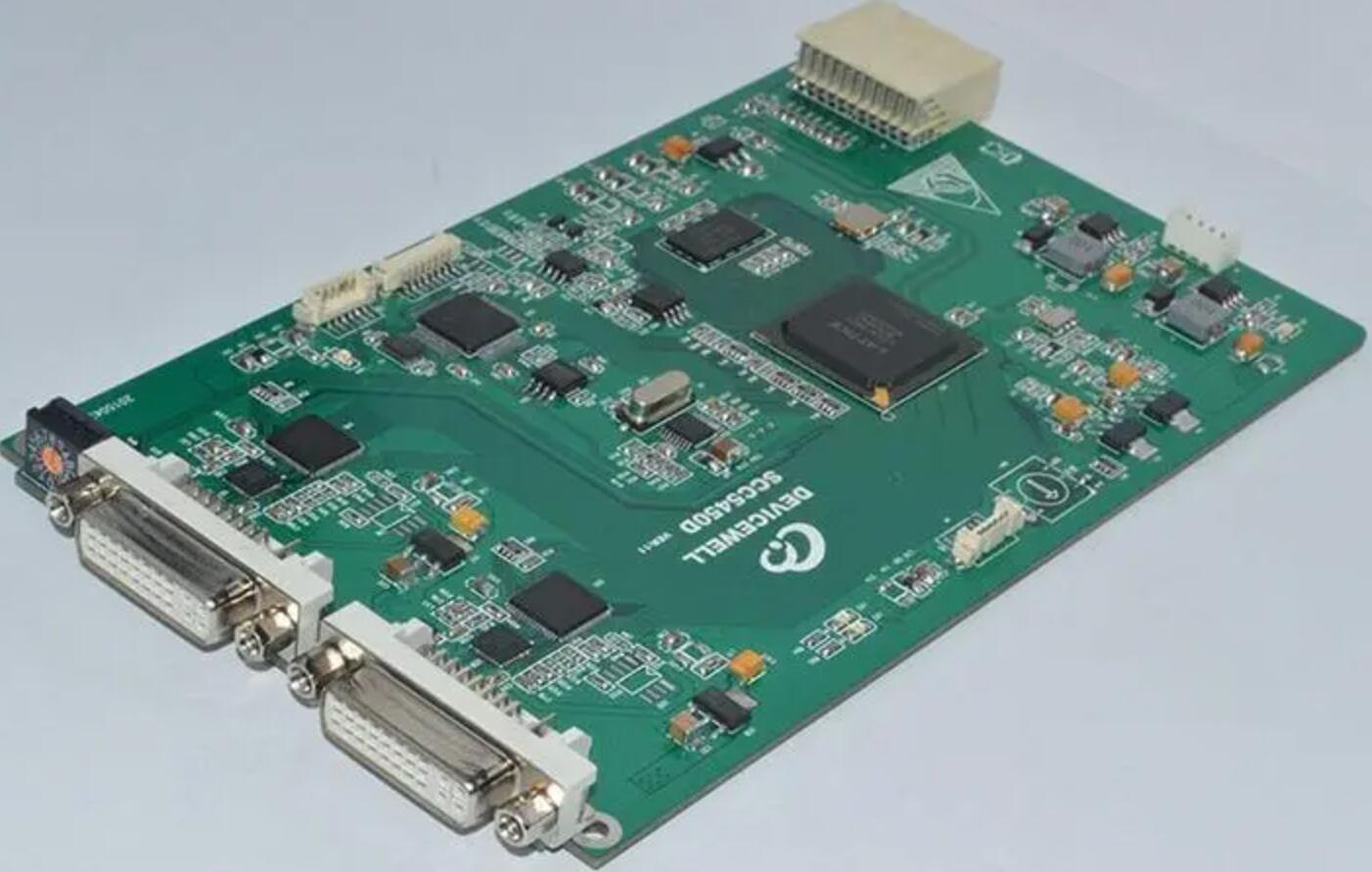
Manufacturing costs are always a major concern for OEMs. Printed circuit board or PCB assembly costs include the materials that go into fabricating them, the components mounted on them, and the expertise necessary to make them reliable and safe. In this article, Hitech PCB analyzes the cost breakup of a PCB assembly, so that our customers can take more informed decisions.
Factors Affecting PCB Assembly
Mechanical size remains one of the major constraints to the design of a PCB. This is because the physical size of a board decides the number of layers in the PCB. The complexity of the circuit and size of components used are also a factor in deciding the size of the board.
The selection of components and the physical size of the board affect the production processes. For instance, the type of components determines via sizes. Fabricating a PCB with large vias may be simpler and less expensive, but fine-pitch and high-density components often require miniature vias. For improving the integrity of the drilling process, fabricators may prefer varying the via sizes across the board.
Other constraints like production timelines and quantities also factor in the final cost of the PCB. Optimizing the manufacturing process often involve the designers into undertaking various processes such as design for assembly, design for fabrication, design for manufacturing, design for excellence, and more. While all these are contributors in improving the reliability, safety, and manufacturing processes involved in fabricating a PCB assembly, they contribute to its final cost.

Meeting DFA and DFM standards ensure the PCB meets physical layout guidelines and capabilities of the manufacturer, while meeting the cost requirements. For instance, DFA determines if the stackup and trace widths match with design rules. DFM improves the collaboration between fabrication and design teams for the board design.
The above factors decide the form factor and physical dimensions of the PCB. The application of the PCB also helps finalize the board size. The actual size of the board may not be a crucial factor for control applications and high-power designs, but it is definitely a factor for a wearable that requires optimal surface area for its PCB.
Minuscule boards may be more expensive on account of higher tolerances, handling, and tooling issues involved in their design and fabrication. Smaller boards require careful handling while fabrication for achieving the allowable tolerances. For proper fabrication and assembly of small boards, fabricators may need to design and build custom jigs and fixtures. For instance, flexible PCBs require supports to minimize the stress on them during the fabrication and assembly processes.
Breakdown of PCB Assembly Factors
Number of Layers and Board Size: Hitech PCB and other board fabricators use a wide range of substrate material sizes. Typically, substrates range from 14 x18 inches to 24 x 30 inches. We commonly use 16 x 18, 18 x 21, 18 x 24, 21 x 24, and 24 x 30 inches. These cover most applications that require large boards to long flex boards. For an 18 x 24 size panel, the usable area will be 16 x 22 inches.
We advise our customers to use the entire space for their circuit. This is because when they use only a section of the board, they are wasting the rest, and the cost is the same. A bigger board always costs more, so customers must make sure their design fits the panel size properly.
The higher the number of copper layers, more is the production cost of the PCB. A complex PCB design must use several vias to connect between different layers, and that increases the cost.
Board Material: For specific board properties like high thermal rating, high Tg, fire retardant materials, low dielectric constant, the cost is going to go up. However, your contract manufacturer may have alternate brands of PCB materials that offer similar properties.
Hitech PCB advises using alternate brands of PCB material against the PCB properties you require in your BOM. This allows the manufacturer more flexibility.
BOM Components: When opting for turnkey projects, the contract manufacturer supplies some or all components. For passive components, we prefer our customers to specify their required specifications, and allow us to use components from alternate manufacturers.
Contract manufacturers maintain an inventory of components that they can offer at a lower price. This way they can use components from stock when customers allow them to use equal or better products in their BOM. They usually buy from reputed suppliers in bulk, and can pass on the price advantage over to customers. Buying a component exclusively for an assembly can be more expensive.
Whether the designer is using SMT or through-hole type components for the PCB assembly is also a factor in deciding its price. Most companies now manufacture SMT components in bulk, and that makes them much cheaper than through-hole components.
Using through-hole components requires drilling the PCB multiple times for each component. The drilling process adds to the cost, while the holes reduce the reliability of the board. Moreover, the presence of through holes reduces the available channels for routing, which can make a complex board much larger. Soldering through-hole components requires wave soldering, a more expensive technology.
Hitech PCB advises all customers to use SMT components, and design the assembly such that all components are on the same side of the board. That simplifies the manufacturing process of the board, reducing its cost.
Design Complexity: Minimizing the complexity of the design reduces the effort at the manufacturer’s end, reducing the cost of the board. For instance, adding a BGA will drive up the costs as it requires extra inspection. Similarly, adding a conformal coating needs an extra assembly step, and adds to the cost.
Standards and Certifications: Conforming to standards and certifications requires a long-term investment from the contract manufacturer, driving up the cost of the PCB. For instance, Hitech PCB makes IPC class III PCBs for aerospace and medical industries. This requires keeping track of various lots we manufacture, sometimes for decades. Furthermore, maintaining certification for compliance to standards like IATF16949, ISO 13485, and ISO 9001 is expensive.
Order Volume and Lead Time: Hitech PCB offers discounts on large volume orders. When we must switch between various low volume jobs, we spend a lot of time in each setup. Therefore, we advise our customers to place their annual orders at a time, rather than ten orders of few assemblies each—we can offer better prices.
Expedited orders are always more expensive. If the lead time for a product is low, it forces the fabricator to source material from suppliers who are more expensive, rather than looking for suppliers who can supply at cheaper rates, but may take more time.
Additional Services: Although contract manufacturers offer several types of services, each of them adds to the cost. For instance, Hitech PCB offers services like design assistance, prototyping, testing, and more.
PCB Assembly Cost Analysis
Broadly, we can break down the total cost of high-volume PCB Assembly into four parts:
Bill of Material Cost — this comprises the bulk of the cost, about 61% of the total.
Cost of PCB material and fabrication — this is about 23% of the total.
Cost of Component Assembly — this is about 13% of the total.
Tooling Costs — this takes up roughly 3% of the total cost.

The breakup shown above is statistical and applicable for high-volume PCB assembly projects. However, not all projects may follow the pattern shown.
Conclusion
Cost analysis of a PCB assembly is helpful when deciding on using methods to reduce its cost. HitechPCB provides our customers complete cost breakup of components and materials, so they can conduct the cost analysis. As shown above, the process is simple once the details are available.
Hitech Circuits Co., Limited is a professional PCB Assembly manufacturer, supplier from

0086-755-29970700
sales@hitechpcb.com; sales@hitechcircuits.com
3F, B5 Dong, Zhimeihuizhi, FuYong, Bao’an Dist. Shenzhen, GuangDong, China 518103
 Chinese
 English
 Russian
 Spanish
 Portuguese


